CDA4101, Assignment 2
Due Sunday, 3/22 (not late until 6 am 3/23)
The homework has 55 points in total.
-
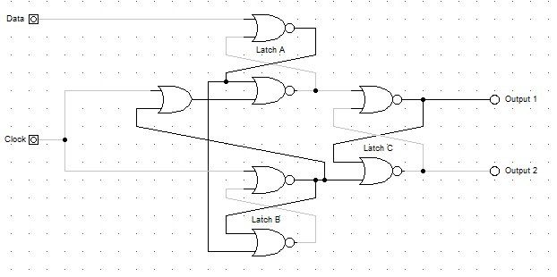
(12 total) Answer these questions about this circuit diagram.
- In terms of the input values for clock and data,
- (2) when will Latch A be in a nondeterministic state (both input lines are 1)?
- (2) when will Latch B be in a nondeterministic state?
- (1) when does Latch C change its state?
- (2) if Output 1 is 0, when does it change to 1?
- (2) if Output 2 is 0, when does it change to 1?
- (2 points) In ten words or less, what is this circuit?

I have created a running example of this circuit using digital works. Download digital works
and my example to run it.
-
(4) On many CPUs there are condition codes to test if the answer was
zero, and to test if there was signed overflow: Z and O. An 8-bit ALU is
constructed from 8 1-bit ALUs in Fig. 3-19. How would each of these condition
codes be wired to such an ALU? Draw the circuits for each. (The O bit is
set when the carry into the highest ALU is different from the carry out of
the highest ALU). Fig. 3-19 is difficult to read. Please refer
to my lecture when I explained the diagram.
-
(3) Calculate the bus bandwidth to display 768x512 full-color video at 30 frames/sec. Assume that
the data must pass over the bus twice, once from the CD-ROM to the memory and once from the memory
to the screen.
-
(2) What is the quiescent state of the S and R inputs to an SR latch built from two NAND gates?
-
(4) The new FIU-PCI Express system has 10 Gbps lanes (gross capacity), in one direction. How many signal wires (not including ground) are needed
in one direction for x32 operation? What is the gross capacity for x32 operation, one way (GBps)? What is the net capacity
one way, assuming 8/10b? What would be the net capacity if 128/130b is used?
-
(6 points) The 4 X 3 memory of Figure 3-29 uses 22 AND gates and three OR
gates. It also has 11 input, output, and control lines.
-
Suppose the circuit were expanded to 64 x 16.
-
How many AND gates would be needed?
-
How many OR gates would be needed?
-
How many pins would be coming into and out of the chip?
-
Suppose the circuit were expanded to 16 x 64.
-
How many AND gates would be needed?
-
How many OR gates would be needed?
-
How many pins would be coming into and out of the chip?
-
(6 total) Refer to the timing diagram of Fig. 3-38. The time needed from the point where !MREQ is asserted and the
data must be stable before it is read can be calculated two ways from the table.
- (2) Calculate the time needed using both calculations for a 100MHz bus.
- (1) If the memory needs 15 nsec for this measurement, how many wait states are needed to read from the memory on a 100MHz bus?
- (2) Calculate the time needed using both calculations for a 200MHz bus.
- (1) If the memory needs 15 nsec for this measurement, how many wait states are needed to read from the memory on a 200MHz bus?
- (6 total) Refer to Figure 3-46. The precharge phase cannot be issued until two full cycles after the last READ or WRITE operation. Using the maximum amount of (legal) pipelining,
- (2) how many bus cycles are needed to read a word from four different rows of bank 0, including the final precharge?
- (2) how many bus cycles are needed to read two words from the same row in bank 0 and two words from the same row in bank 1, including the final precharges?
- (2) how many bus cycles are needed to read one word from each of the four banks, including the final precharges?
-
(3) Assume DMA is being used to read all 2048 sectors of 512-bytes each in a track on a disk.
Each 32-bit DMA transfer takes 1 bus cycle of 5 nsec. It takes one rotation of 8 msec to
read the entire track. How many cycles per millisecond is the DMA using the bus (and cycle stealing from the CPU)?
-
(3) The new FIU-USB has a maximum payload of 3,200,000 bits for an isochronous data packet.
Assuming that a device may send only one data packet per frame, what is the maximum
bandwidth (in MBps) for a sinlge isochronous device?
-
(6) In section 3.7.2, assume that the memory space is 32K; the EPROM is
2K in size and will be placed at address 18K; the RAM is 4k in size and
will be placed at address 26K; the PIO is 4 bytes and will be placed starting
at address 7K. Draw the circuit for the !CS lines into the devices. Use
full address decoding.
